- 您现在的位置:买卖IC网 > Sheet目录308 > ADZS-21469-EZLITE (Analog Devices Inc)KIT EVAL EZ LITE ADSP-21469
�� �
�
�ADSP-21462/ADSP-21465/ADSP-21467/ADSP-21469�
�Preliminary� Technical� Data�
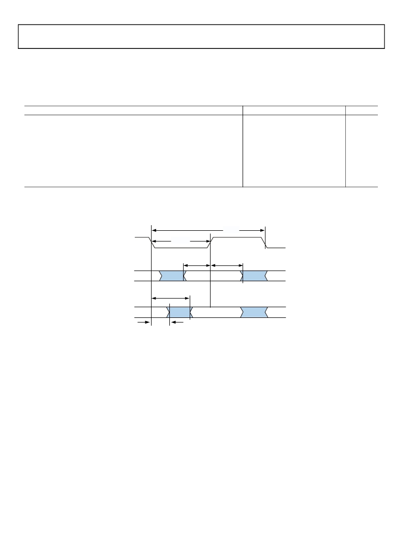
�Sample� Rate� Converter—Serial� Output� Port�
�For� the� serial� output� port,� the� frame-sync� is� an� input� and� it�
�should� meet� setup� and� hold� times� with� regard� to� SCLK� on� the�
�output� port.� The� serial� data� output,� SDATA,� has� a� hold� time�
�Table� 37.� ASRC,� Serial� Output� Port�
�and� delay� specification� with� regard� to� SCLK.� Note� that� SCLK�
�rising� edge� is� the� sampling� edge� and� the� falling� edge� is� the�
�drive� edge.�
�Parameter�
�Min�
�Max�
�Unit�
�Timing� Requirements�
�t� SRCSFS� 1�
�t� SRCHFS� 1�
�t� SRCCLKW�
�t� SRCCLK�
�FS� Setup� Before� SCLK� Rising� Edge�
�FS� Hold� After� SCLK� Rising� Edge�
�Clock� Width�
�Clock� Period�
�TBD�
�TBD�
�TBD�
�TBD�
�TBD�
�TBD�
�TBD�
�TBD�
�ns�
�ns�
�ns�
�ns�
�Switching� Characteristics�
�TBD�
�TBD�
�t� SRCTDD� 1�
�Transmit� Data� Delay� After� SCLK� Falling� Edge�
�TBD�
�TBD�
�ns�
�t� SRCTDH�
�1�
�Transmit� Data� Hold� After� SCLK� Falling� Edge�
�TBD�
�TBD�
�ns�
�1�
�AMI_DATA,� SCLK,� and� FS� can� come� from� any� of� the� DAI� pins.� SCLK� and� FS� can� also� come� via� PCG� or� SPORTs.� PCG’s� input� can� be� either� CLKIN� or� any� of� the� DAI� pins.�
�S� AMPLE� EDGE�
�t� S� RCCLK�
�DAI_P20� -� 1�
�(� S� CLK)�
�t� S� RCCLKW�
�t� S� RC� S� F� S�
�t� S� RCHF� S�
�DAI_P20� -� 1�
�(F� S� )�
�t� S� RCTDD�
�DAI_P20� -� 1�
�(� S� DATA)�
�t� S� RCTDH�
�Figure� 26.� ASRC� Serial� Output� Port� Timing�
�Rev.� PrC�
�|� Page� 40� of� 62� |� January� 2009�
�发布紧急采购,3分钟左右您将得到回复。
相关PDF资料
ADZS-21479-EZLITE
KIT EVAL EZ BOARD ADSP-2147X
ADZS-21489-EZLITE
KIT EVAL EZ BOARD ADSP-2148X
ADZS-218X-ICE-2.5V
EMULATOR SRL FOR ADDS-218X-ICE
ADZS-BF506F-EZLITE
KIT EVAL EZLITE ADSP-BF506F
ADZS-BF518F-EZLITE
KIT EZ LITE BF512F/14F/16F/18F
ADZS-BF527-EZLITE
BOARD EVAL ADSP-BF527
ADZS-BF533-EZLITE
KIT W/BOARD EVAL FOR ADSP-BF533
ADZS-BF538F-EZLITE
BOARD EVAL FOR ADSP-BF538
相关代理商/技术参数
ADZS-21479-EZBRD
功能描述:BOARD EVAL FOR ADZS-2147X RoHS:是 类别:编程器,开发系统 >> 通用嵌入式开发板和套件(MCU、DSP、FPGA、CPLD等) 系列:SHARC® 标准包装:1 系列:PICDEM™ 类型:MCU 适用于相关产品:PIC10F206,PIC16F690,PIC16F819 所含物品:板,线缆,元件,CD,PICkit 编程器 产品目录页面:659 (CN2011-ZH PDF)
ADZS-21479-EZBRD
制造商:Analog Devices 功能描述:EZ BOARD SUPPORTING SHARC 21479
ADZS-21479-EZLITE
功能描述:KIT EVAL EZ BOARD ADSP-2147X RoHS:是 类别:编程器,开发系统 >> 通用嵌入式开发板和套件(MCU、DSP、FPGA、CPLD等) 系列:SHARC® 产品培训模块:Blackfin® Processor Core Architecture Overview
Blackfin® Device Drivers
Blackfin® Optimizations for Performance and Power Consumption
Blackfin® System Services 特色产品:Blackfin? BF50x Series Processors 标准包装:1 系列:Blackfin® 类型:DSP 适用于相关产品:ADSP-BF548 所含物品:板,软件,4x4 键盘,光学拨轮,QVGA 触摸屏 LCD 和 40G 硬盘 配用:ADZS-BFBLUET-EZEXT-ND - EZ-EXTENDER DAUGHTERBOARDADZS-BFLLCD-EZEXT-ND - BOARD EXT LANDSCAP LCD INTERFACE 相关产品:ADSP-BF542BBCZ-4A-ND - IC DSP 16BIT 400MHZ 400CSBGAADSP-BF544MBBCZ-5M-ND - IC DSP 16BIT 533MHZ MDDR 400CBGAADSP-BF542MBBCZ-5M-ND - IC DSP 16BIT 533MHZ MDDR 400CBGAADSP-BF542KBCZ-6A-ND - IC DSP 16BIT 600MHZ 400CSBGAADSP-BF547MBBCZ-5M-ND - IC DSP 16BIT 533MHZ MDDR 400CBGAADSP-BF548BBCZ-5A-ND - IC DSP 16BIT 533MHZ 400CSBGAADSP-BF547BBCZ-5A-ND - IC DSP 16BIT 533MHZ 400CSBGAADSP-BF544BBCZ-5A-ND - IC DSP 16BIT 533MHZ 400CSBGAADSP-BF542BBCZ-5A-ND - IC DSP 16BIT 533MHZ 400CSBGA
ADZS-21489-EZBRD
功能描述:BOARD EVAL FOR ADZS-2148X RoHS:是 类别:编程器,开发系统 >> 通用嵌入式开发板和套件(MCU、DSP、FPGA、CPLD等) 系列:SHARC® 产品培训模块:Blackfin® Processor Core Architecture Overview
Blackfin® Device Drivers
Blackfin® Optimizations for Performance and Power Consumption
Blackfin® System Services 特色产品:Blackfin? BF50x Series Processors 标准包装:1 系列:Blackfin® 类型:DSP 适用于相关产品:ADSP-BF548 所含物品:板,软件,4x4 键盘,光学拨轮,QVGA 触摸屏 LCD 和 40G 硬盘 配用:ADZS-BFBLUET-EZEXT-ND - EZ-EXTENDER DAUGHTERBOARDADZS-BFLLCD-EZEXT-ND - BOARD EXT LANDSCAP LCD INTERFACE 相关产品:ADSP-BF542BBCZ-4A-ND - IC DSP 16BIT 400MHZ 400CSBGAADSP-BF544MBBCZ-5M-ND - IC DSP 16BIT 533MHZ MDDR 400CBGAADSP-BF542MBBCZ-5M-ND - IC DSP 16BIT 533MHZ MDDR 400CBGAADSP-BF542KBCZ-6A-ND - IC DSP 16BIT 600MHZ 400CSBGAADSP-BF547MBBCZ-5M-ND - IC DSP 16BIT 533MHZ MDDR 400CBGAADSP-BF548BBCZ-5A-ND - IC DSP 16BIT 533MHZ 400CSBGAADSP-BF547BBCZ-5A-ND - IC DSP 16BIT 533MHZ 400CSBGAADSP-BF544BBCZ-5A-ND - IC DSP 16BIT 533MHZ 400CSBGAADSP-BF542BBCZ-5A-ND - IC DSP 16BIT 533MHZ 400CSBGA
ADZS-21489-EZBRD
制造商:Analog Devices 功能描述:EZ BOARD SUPPORTING SHARC 21489
ADZS-21489-EZLITE
功能描述:KIT EVAL EZ BOARD ADSP-2148X RoHS:是 类别:编程器,开发系统 >> 通用嵌入式开发板和套件(MCU、DSP、FPGA、CPLD等) 系列:SHARC® 产品培训模块:Blackfin® Processor Core Architecture Overview
Blackfin® Device Drivers
Blackfin® Optimizations for Performance and Power Consumption
Blackfin® System Services 特色产品:Blackfin? BF50x Series Processors 标准包装:1 系列:Blackfin® 类型:DSP 适用于相关产品:ADSP-BF548 所含物品:板,软件,4x4 键盘,光学拨轮,QVGA 触摸屏 LCD 和 40G 硬盘 配用:ADZS-BFBLUET-EZEXT-ND - EZ-EXTENDER DAUGHTERBOARDADZS-BFLLCD-EZEXT-ND - BOARD EXT LANDSCAP LCD INTERFACE 相关产品:ADSP-BF542BBCZ-4A-ND - IC DSP 16BIT 400MHZ 400CSBGAADSP-BF544MBBCZ-5M-ND - IC DSP 16BIT 533MHZ MDDR 400CBGAADSP-BF542MBBCZ-5M-ND - IC DSP 16BIT 533MHZ MDDR 400CBGAADSP-BF542KBCZ-6A-ND - IC DSP 16BIT 600MHZ 400CSBGAADSP-BF547MBBCZ-5M-ND - IC DSP 16BIT 533MHZ MDDR 400CBGAADSP-BF548BBCZ-5A-ND - IC DSP 16BIT 533MHZ 400CSBGAADSP-BF547BBCZ-5A-ND - IC DSP 16BIT 533MHZ 400CSBGAADSP-BF544BBCZ-5A-ND - IC DSP 16BIT 533MHZ 400CSBGAADSP-BF542BBCZ-5A-ND - IC DSP 16BIT 533MHZ 400CSBGA
ADZS-2189M-EZLITE
功能描述:开发板和工具包 - 其他处理器 ADZS-2189M-EZLITE
RoHS:否 制造商:Freescale Semiconductor 产品:Development Systems 工具用于评估:P3041 核心:e500mc 接口类型:I2C, SPI, USB 工作电源电压:
ADZS-218X-ICE-2.5V
功能描述:EMULATOR SRL FOR ADDS-218X-ICE RoHS:是 类别:编程器,开发系统 >> 内电路编程器、仿真器以及调试器 系列:EZ-ICE® 产品变化通告:Development Systems Discontinuation 19/Jul/2010 标准包装:1 系列:* 类型:* 适用于相关产品:* 所含物品:*